Application
半導體先進封裝
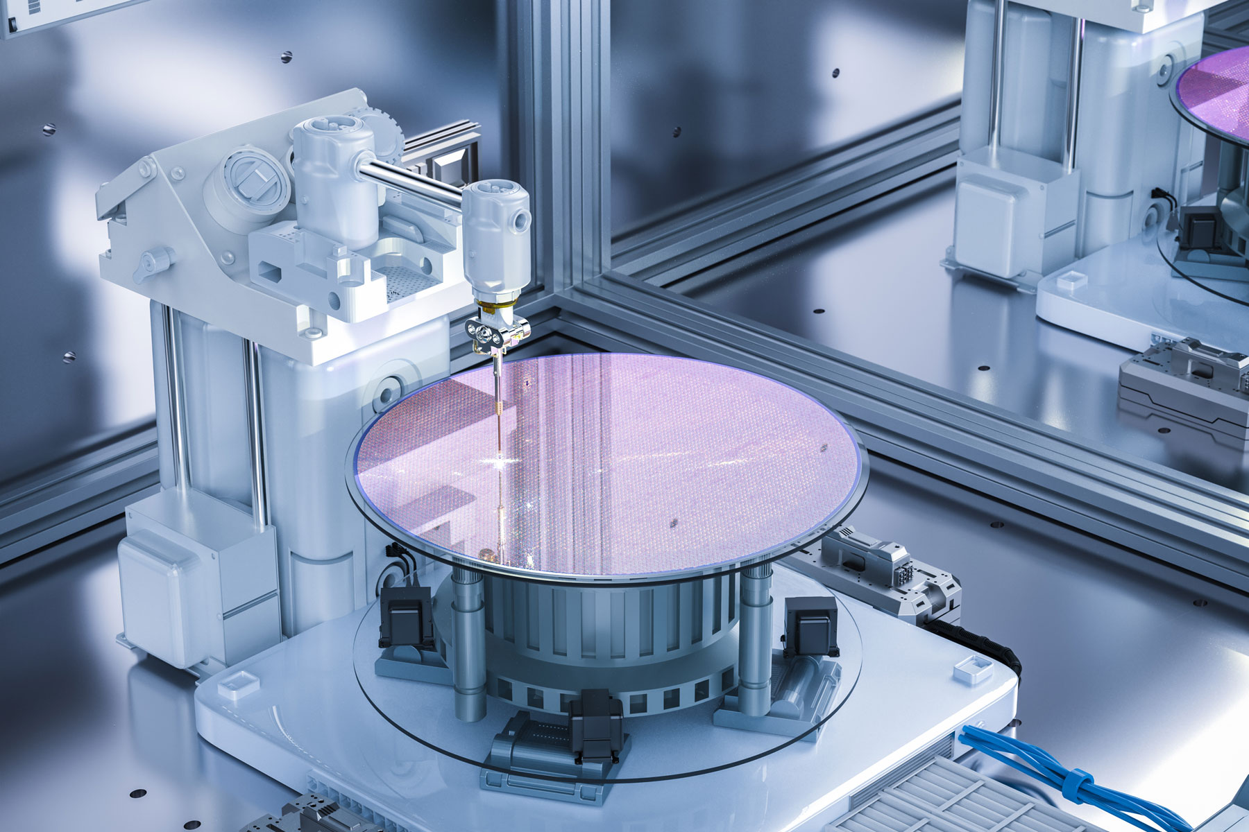
隨著摩爾定律(Moore’s Law) 放緩,晶片微縮成本急劇上升,業界開始藉由系統級封裝(SiP, System-in-Package)與晶片堆疊(3D IC)等技術,在封裝層面提升運算效能與功能密度。先進封裝由多元件整合為一體來縮短訊號路徑,主要利用重佈線(RDL, Redistribution Layer)和矽穿孔技術(TSV, Through Silicon Via)使各式元件彼此之間進行連接來提高整體效能。
傳統封裝的著重於保護晶片、導出訊號與散熱,而先進封裝更進一步在實現晶片間的高密度整合與高效能互連。先進封裝包含多晶片模塊、3D IC、2.5D IC、異構集成、扇出晶圓級封裝、系統級封裝、絎縫封裝、將處理器和存儲器組合在單個封裝中、晶片堆疊、封裝中的多個芯粒或晶片、這些技術的組合等等。
隨著AI運算所需的高階伺服器應用,市場普遍預測先進封裝的年複合成長率為7%~8%,高於傳統封裝之2%~3%,未來將繼續成為半導體發展的主軸。

Schematics of 2.5D package

(a) The top view of chip-on wafer and
(b) chip-on-TSI-on-substrate

Ref : Heterogeneous 2.5D integration on through silicon interposer
Other Product
其他產品
https://pttech.morcept.tw/wp-content/uploads/2026/02/scientific-research-laboratory-new-cpu-chip-test-development.jpg
1281
1920
agent22
/wp-content/uploads/2025/12/PTLOGO.png
agent222026-02-03 12:40:362026-02-03 16:17:26碳化矽專利
https://pttech.morcept.tw/wp-content/uploads/2026/02/computer-printed-circui.jpg
1280
1920
agent22
/wp-content/uploads/2025/12/PTLOGO.png
agent222026-02-03 12:27:062026-02-03 16:16:33碳化矽加工
https://pttech.morcept.tw/wp-content/uploads/2026/02/scientist-hands-gloves-work-with-circuit-board-laboratory-close-up-view.jpg
1281
1920
agent22
/wp-content/uploads/2025/12/PTLOGO.png
agent222026-02-03 12:10:422026-02-03 12:26:33代工服務
https://pttech.morcept.tw/wp-content/uploads/2026/02/IMAG0161.jpg
538
900
agent22
/wp-content/uploads/2025/12/PTLOGO.png
agent222026-02-03 11:19:362026-02-03 16:16:53功能鍍膜
https://pttech.morcept.tw/wp-content/uploads/2025/12/圖片_20251017130751_15_8.jpg
899
900
agent22
/wp-content/uploads/2025/12/PTLOGO.png
agent222026-02-03 11:01:452026-02-03 11:57:16散熱鍍膜
https://pttech.morcept.tw/wp-content/uploads/2025/12/modern-3d-printer-printing-figure-close-up-automatic-three-dimensional-3d-printer-performs-plastic-modeling-laboratory-blue-gray-color.jpg
1247
1920
agent22
/wp-content/uploads/2025/12/PTLOGO.png
agent222025-12-18 17:22:292026-02-03 11:57:11設備與技術服務
https://pttech.morcept.tw/wp-content/uploads/2025/12/abstract-black-background-with-patterned-glass-texture.jpg
600
900
agent22
/wp-content/uploads/2025/12/PTLOGO.png
agent222025-12-18 13:57:132026-02-03 11:11:46散熱材料
