
Application
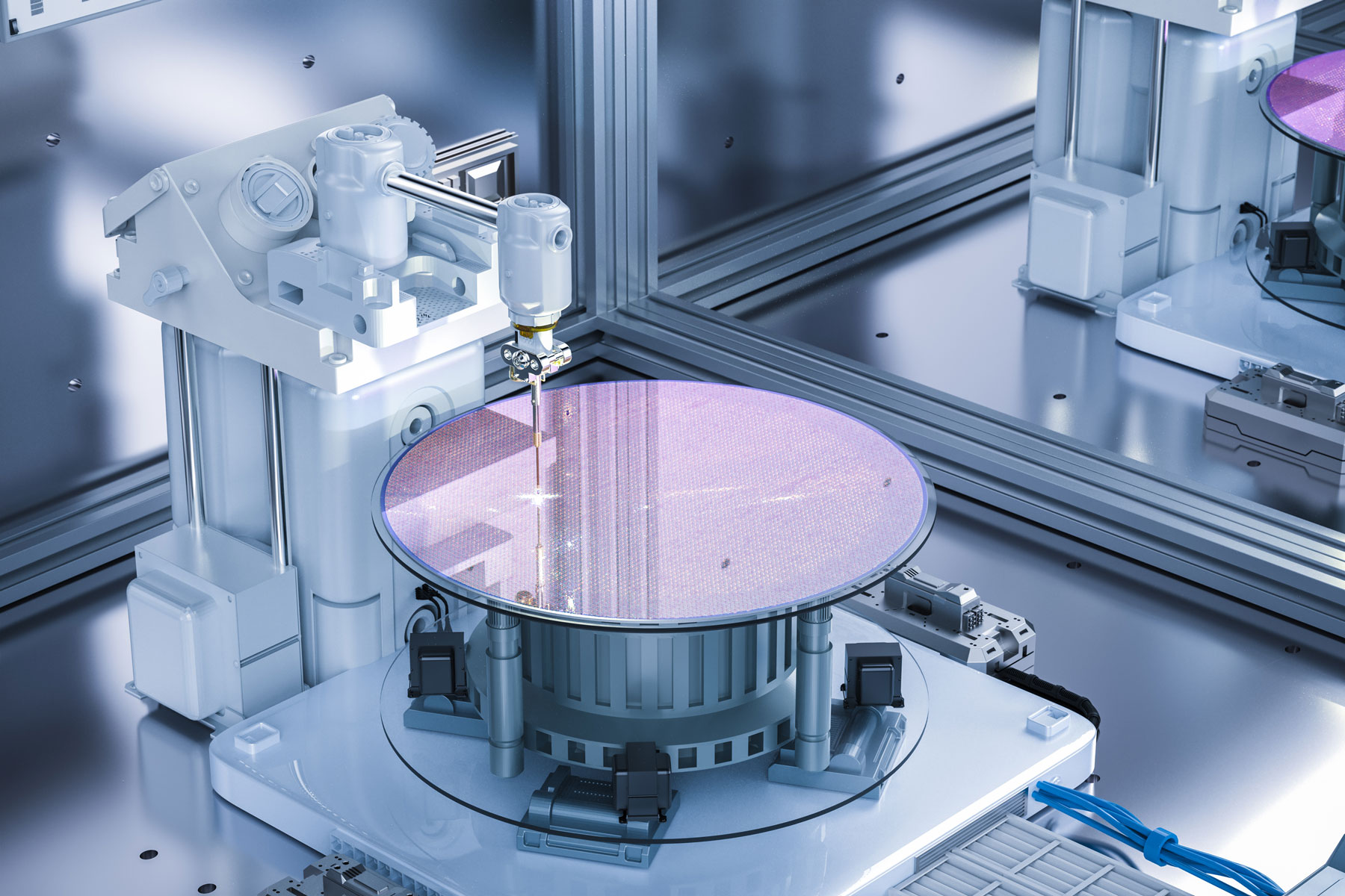
As Moore’s Law slows and the cost of further node scaling rises sharply, the industry is increasingly turning to packaging-level techniques such as System-in-Package (SiP) and 3D IC chip stacking to raise compute performance and functional density. Advanced packaging—integrating multiple components into a single package—has become a key route to sustaining semiconductor performance growth.
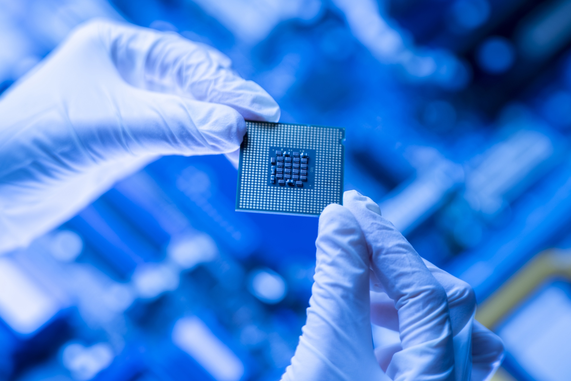
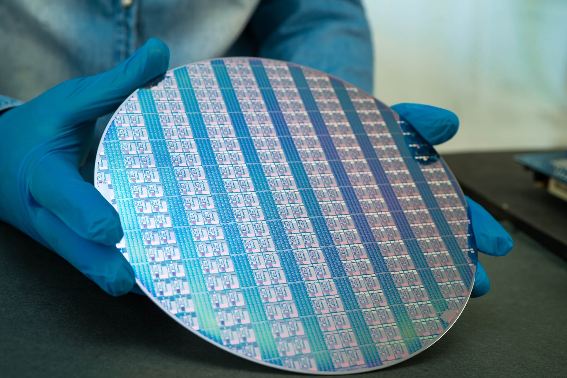
Conventional packaging focuses on protecting the die, routing signals, and dissipating heat; advanced packaging goes further, enabling high-density integration and high-performance interconnect between dies. It encompasses multi-chip modules, 3D IC, 2.5D IC, heterogeneous integration, fan-out wafer-level packaging (Fan-out WLP), System-in-Package (SiP), and chip-on-wafer-on-substrate (CoWoS), combining processors and memory in a single package to shorten interconnect distance.
Driven by AI computing for high-end server applications, the market broadly expects advanced packaging to grow at a CAGR of 7%–8%, higher than the 2%–3% for conventional packaging, and to remain a central axis of semiconductor development.

Schematics of 2.5D package
 The top view of chip-on wafer and (b) chip-on-TSI-on-substrate")
(a) The top view of chip-on wafer and (b) chip-on-TSI-on-substrate

CoC-First assembly: (a) before reflow and (b) after reflow (Courtesy of Institute of Microelectronics).
Ref : Heterogeneous 2.5D integration on through silicon interposer