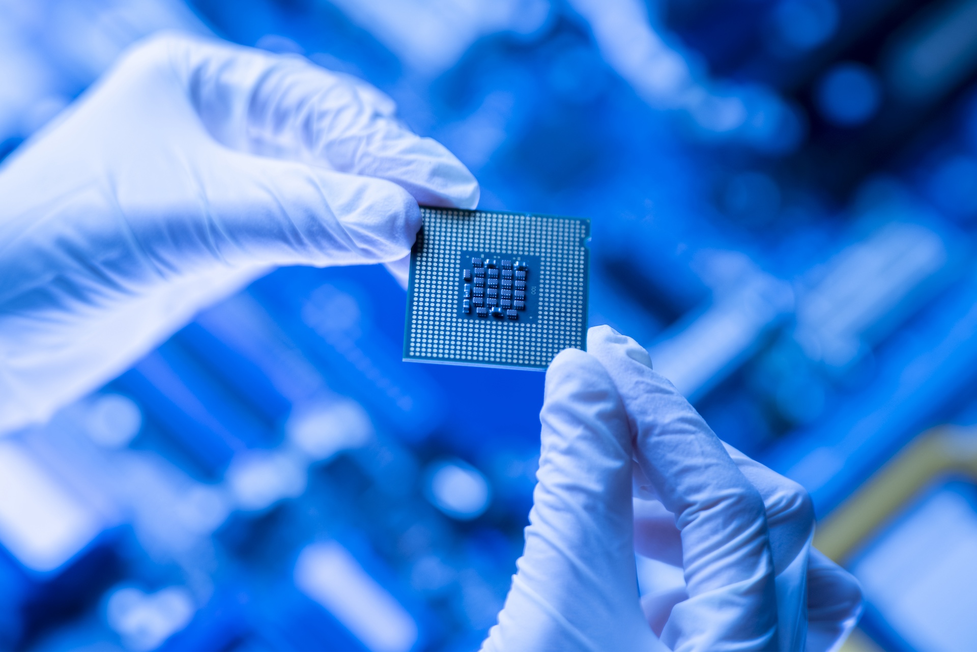

Drawing on deep compound-semiconductor R&D, JingCheng Materials has built end-to-end technology coverage — from seed development and key-equipment optimization to volume-production processing. We deliver high-quality, low-defect and highly consistent SiC substrates as a rock-solid core solution for power electronics, automotive semiconductors, AI thermal management, and high-frequency communications industries worldwide.
1. Core Crystal Growth: 8-inch Volume Production Leadership and 12-inch Forward Roadmap
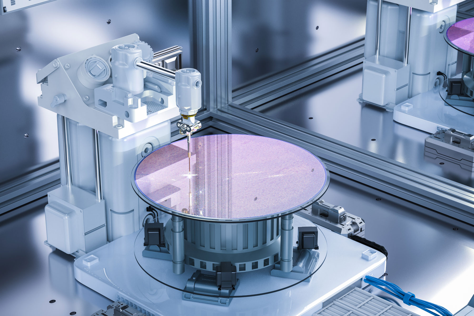
JingCheng has deep expertise in PVT (Physical Vapor Transport). Through precise control of thermal/flow fields and dynamics, we have crossed generational boundaries from 6″ to 8″ to 12″ wafer sizes.
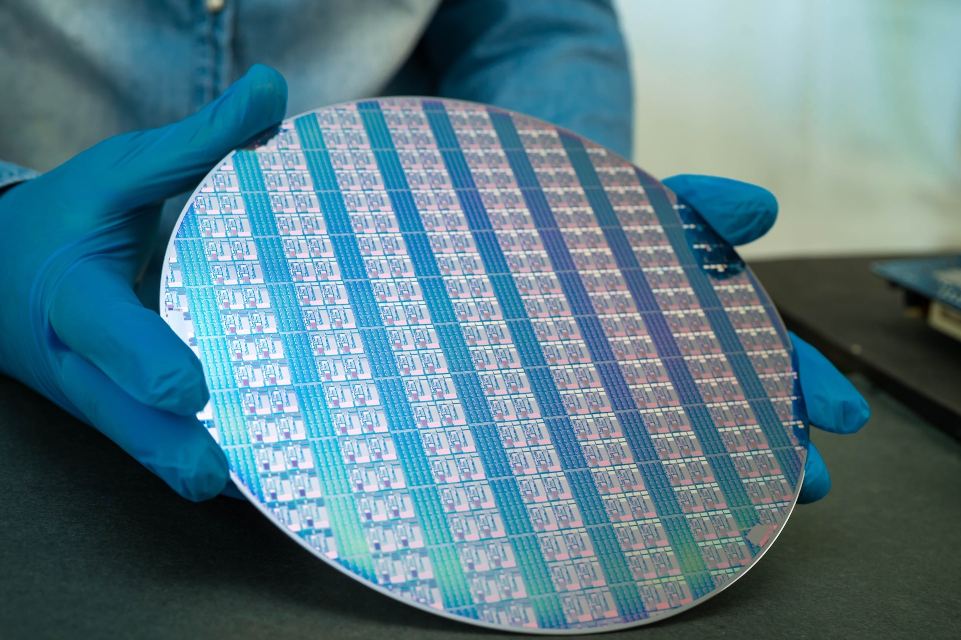
8-inch conductive crystal volume production
We have completed crystal-growth process development for both Conductive and Semi-insulating SiC at 6″ and 8″. 8″ conductive crystals are now in volume production with excellent yield and capacity, meeting global downstream demand for large-format, cost-effective substrates.12-inch forward R&D
Responding to the industry’s relentless pursuit of higher output and lower cost, JingCheng has pioneered R&D on 12″ (300 mm) SiC crystal growth. Active development and key testing are underway, demonstrating our strong R&D capability and reserves in large-format compound semiconductor materials.In-house key equipment
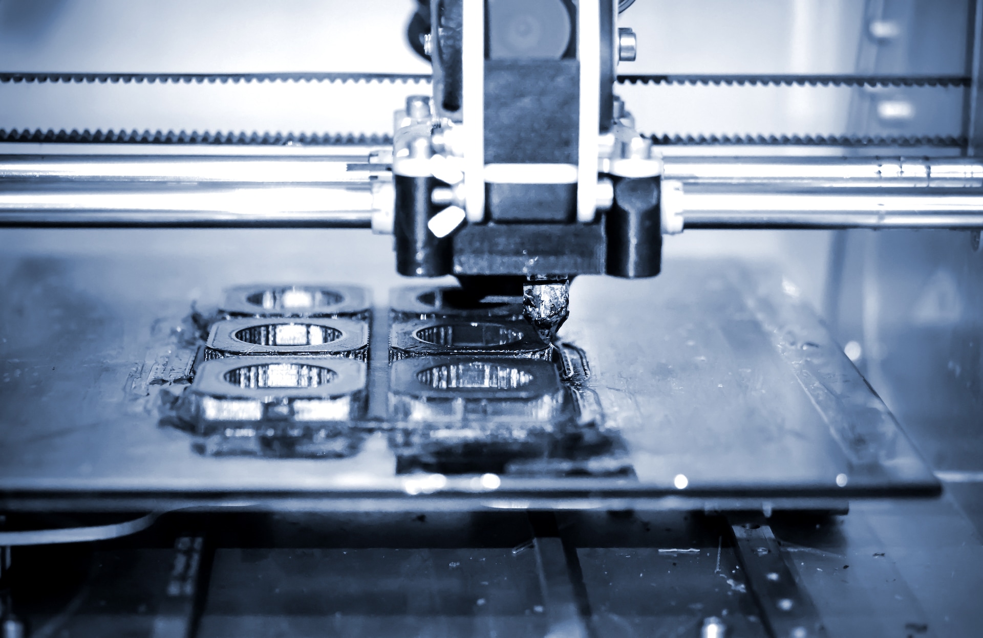
Our engineering team designs and optimizes crystal-growth equipment in-house, addressing process bottlenecks in 8″ volume production and 12″ R&D in real time and ensuring excellent thickness and quality consistency at large diameters.End-to-end process coverage
Mastering both conductive and semi-insulating growth, we flexibly supply diverse high-end markets — power electronics and RF communications — with the most complete technical support.
2. Vertically Integrated One-Stop Production
JingCheng has built a complete R&D center and production base in Taiwan, closing the quality loop from source to finished product.
In-house seed crystals
We control SiC substrates’ “quality DNA” — through proprietary high-quality seed technology we govern crystal orientation and defects from the source, ensuring excellent consistency in every substrate.End-to-end processing
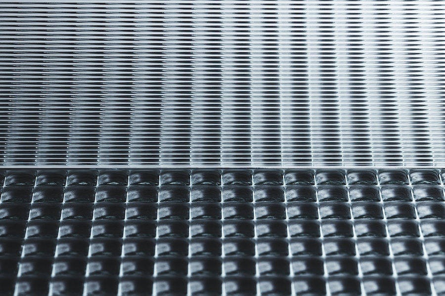
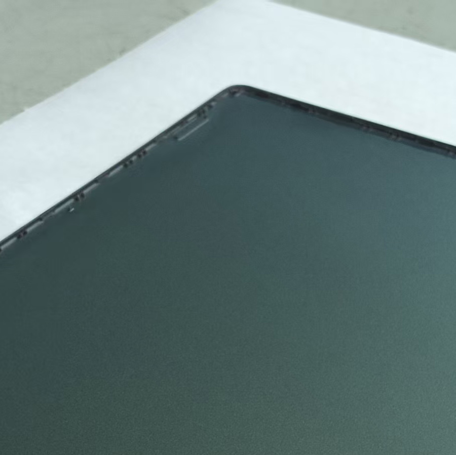
We integrate growth, slicing, grinding and polishing. With this one-stop vertical integration we precisely manage every step from boule to substrate processing, delivering the highest-standard surface quality.
3. Rigorous Quality Management: Aligned with Automotive-Grade International Standards
We treat defect control as the core of our competitive edge. Through systematic management and cutting-edge inspection, we ensure products meet stringent industrial- and automotive-grade standards.
International certifications
We are certified to ISO 9001:2015 and are actively building an IATF 16949 automotive quality system,working to become a trusted partner in the global automotive electronics supply chain.Ultimate defect control (TSD/BPD)
Through optimized process parameters, we strictly control TSD (threading screw dislocations) and BPD (basal plane dislocations) density, significantly improving downstream power devices’ breakdown voltage and long-term reliability.High purity and consistency
Using state-of-the-art analytical instruments to monitor physical and electrical characteristics, we ensure uniform, excellent electrical performance across large-format substrates.