
High Aspect-Ratio Glass-Substrate Via-Fill Electroplating and Inspection Technology

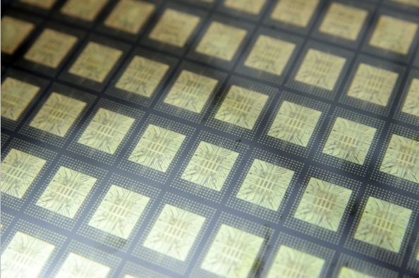
ITRI’s “High Aspect-Ratio Glass-Substrate Via-Fill Electroplating and Inspection Technology” effectively increases electrode density and improves chip stacking, helping Taiwan’s semiconductor industry continue to lead. The image depicts advanced fan-out packaging—a domain where this technology can be applied.
Glass-Interposer technology brings 2D-to-3D advanced packaging with more stable yields and more competitive cost. As semiconductor processes continue to advance, the aspect ratio of vias linking layers keeps increasing. ITRI’s “High Aspect-Ratio Glass-Substrate Via-Fill Electroplating and Inspection Technology” effectively raises electrode density and improves chip stacking, helping Taiwan’s semiconductor industry stay ahead—earning ITRI’s Outstanding Research Gold Award.
With the 5G era and the rise of AI, IoT, and connected vehicles, semiconductors continue to scale to 7 and 5 nm—and toward 3 and 2 nm—nearing Moore’s-Law limits, driving the need for new routes. Heterogeneous integration, which stacks different electronic components into a single chip via 2.5D or 3D design, has emerged as a key breakthrough.
Leading technology—world’s highest aspect ratio
Traditional 2D packaging mounts chips side-by-side on a single plane. As chips trend toward thinner, lighter, smaller—while requiring more compute and lower power—2D packaging can no longer meet industry demand. 3D packaging breaks the horizontal constraint by vertically stacking different-function chips via heterogeneous integration, dramatically boosting module compute capability.
Interposer technology is one key to heterogeneous integration. Glass interposers offer low warpage, faster signal transmission, and better power efficiency—and they meet thin-and-light requirements, making them an increasingly favored option. Interposers require metal interconnects between layers, so vias are drilled in the glass. As processes advance, the via aspect ratio (AR) continues to grow.
“Aspect ratio” (also called depth-to-width ratio) is the ratio of via depth to diameter. Huang Meng-Chi, deputy general director of ITRI’s Mechanical and Mechatronics Systems Research Laboratories (Advanced Mechanical Technology Division), explains: with more 3D stacking layers, vias must go deeper; as chip sizes and line/space shrink, via diameters shrink too. Small-diameter, high-AR vias are therefore an inevitable trend—but the higher the AR, the harder the process, a key challenge for the industry.
“It’s like constructing a high-rise: floors are stacked, and the glass substrate is the floor between levels. You must drill through to connect circuits and pipes between floors so utilities flow normally,” Huang explained.
Over five years, ITRI led the world in developing this technology. Through-Glass Vias (TGVs) connect upper and lower metal traces, transmitting power and signals to optimize chip performance. “ITRI’s technology ensures signal and power quality even as ‘the building’ gets taller,” Huang said.
Wet metal-plating deposition—achieving the highest AR
Many international teams research high AR, but most reach only AR 10—far short of ITRI’s solution. ITRI’s lead rests on three key technologies. First, a brand-new via-fill electroplating process: a glass through-via substrate serves as the interposer, with copper plated to fill the vias and connect upper and lower circuits. To improve metal-glass adhesion, a 100–200 nm composite oxide conductive thin film is formed on the glass surface before filling, acting as a bonding bridge.
Industry typically forms this film via dry-plus-wet processes—using PVD vacuum plasma deposition to drive metal ions into the via. But more stacked layers means deeper vias, making precise filling harder and lowering yield. ITRI developed a low-cost composite oxide conductive thin film suitable for high AR using an all-wet process: by immersing in inorganic-oxide and electroless-copper solutions that flow through the deep vias, an oxide film forms on the surface; a low-temperature co-firing step creates intermetallic compounds between the metal-oxide film and the glass, overcoming the poor glass-metal adhesion barrier.
“With traditional processes, AR 15 is the limit,” Huang said. The all-wet process achieves AR 15–30, with seed-layer deposition rates above 70% and good coverage. Given the high cost of PVD tools, switching from dry-plus-wet to all-wet equipment can save about 50% in cost—meaningful relief for manufacturers.
Single-agent, dual-function plating additive—seamless fill
The second highlight is the development of a single-agent, dual-function via-fill plating additive. Normally, when filling vias with copper, plating is fastest at the surface and slowest at the center, causing voids; under high currents these voids cause rapid chip failures. Special additives are therefore used to slow plating at the via mouth so the center fills first, before the mouth closes—reducing voids.
To solve this, industry commonly uses three additives at once; but each is consumed at a different rate and must be replenished, and they interfere with one another—making it hard to know what or how much to add. The team chose to develop a new additive from scratch: “starting with literature surveys to identify chemicals that might meet the functional needs, then screening one by one,” Huang said.
After exploration, the team identified several candidates and ran formulation experiments. Lead developer Chang Yu-Hsiang (ITRI Mechanical & Mechatronics) spent six months almost daily in the lab, meticulously recording each step, and carefully chose a chemical never before used in electroplating—surprisingly possessing both suppression and leveling functions, with excellent results even on its own. “As a single-agent via-fill plating, it not only solves coverage issues but also reduces measurement interference from multiple additives, improving process stability and yield. Compared with current industry formulations, it can save 50% in cost,” Huang said excitedly.
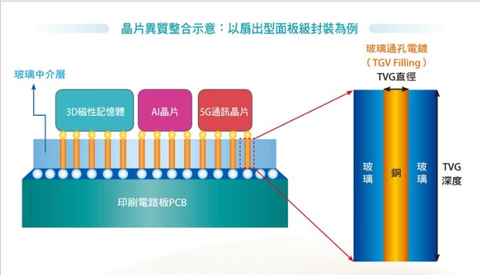
Schematic of chip heterogeneous integration—fan-out panel-level packaging as an example.
3D micro-void inspection—nowhere for defects to hide
The third highlight is an advanced 3D Sphere-Fitting algorithm for inspecting high-AR copper via fills. Huang noted that this was the most challenging and difficult part of the development. Structures and chemistries can be tuned by the team, but only direct inspection reveals whether vias are properly filled from edge to center, or where voids hide—visible to neither the naked eye nor conventional microscopes. “Skipping inspection is like developing blindfolded—you can’t improve.”
Initially the team outsourced inspections; each substrate took half a day, and 3D X-rays required manual checks; iterating on multiple formulations could take 1–2 weeks. Fortunately, in-house materials experts pitched in to develop an enhanced 3D sphere-fitting algorithm. Using high-resolution, high-contrast nano-tomography, software analyzes micro-void distributions and diameters within the structure to find defects quickly and accurately. “Its biggest breakthrough is the ability to inspect hundreds of TGV copper fills simultaneously, returning results in 1–2 days—greatly reducing inspection and correction time,” Huang said.
Dr. Lin Tzu-Hung, ITRI Materials and Chemical Research Laboratories, noted that similar void-detection techniques are used in biomedical materials and oil exploration—e.g., dental dentin microtubules and petroleum reservoir analysis. Applying automated void detection with nano-CT 3D inspection in the electronics industry is a first, and a new attempt for materials. “The challenge is that copper scatters X-rays, so software must remove noise and scatter to build a clear 3D axis. Once defined, the program quickly and automatically identifies the position, axial orientation, and locations of voids and defects within the metal columns. With precise coordinates, electron microscopes can then confirm at higher resolution, guiding corrections,” Lin said.
Through accurate inspection, the team felt their progress. “In early days, technology was less refined—voids were huge, like cracks down the middle of a baseball bat. As we refined the process, voids shrank to peanut-sized holes 2–4 μm across; today we can’t even find any voids,” Huang said with a satisfied smile.
Strategic preparation for the semiconductor industry—generating NT$100B+ value
This technology applies to fan-out panel-level packaging (FOPLP), HDI PCBs, and IC substrates, meeting the needs of advanced electronics processes. Huang noted that although the technology covers only part of the packaging process, key developments such as wet equipment and the single-agent additive shorten cycle time and save manufacturers at least 30% in equipment and chemical costs—estimated to create hundreds of billions of NT$ in value.
Another significance is enabling cross-industry collaboration: a globally known glass supplier traditionally focused on displays expanded into semiconductors through this project, gaining a new product direction; meanwhile, two Taiwanese equipment makers partnering with ITRI on chemicals and tools entered advanced semiconductor packaging equipment for the first time, building next-gen domestic equipment capability.
Huang revealed that current industry production requirements call for AR ~7–8, expected to rise to 10–15 in 2–3 years—ITRI is preparing the industry ahead of time. Pilot testing is under way at major OSAT facilities, and the team continues to refine the technology, hoping for early mass production to land innovation in Taiwan and maintain the semiconductor industry’s leading edge.
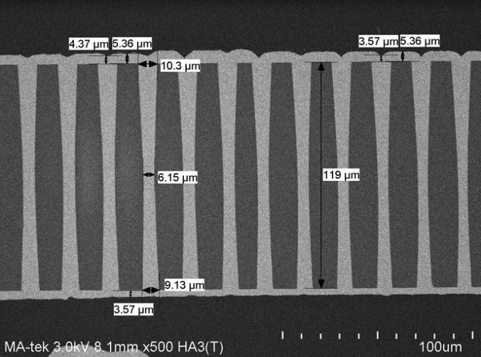
Cross-section SEM of high-AR plated via fill: 10 µm opening, ~120 µm depth, 3.5–5.3 µm surface copper, AR ~12—surpassing industry levels.
Source:
ITRI, Industrial Technology and Information Monthly.