
Industry Technology and Application Trends of Silicon Carbide Modules
Silicon-based power devices and modules are reaching a performance ceiling in high-power applications, prompting scientists to explore materials and technologies among compound semiconductors. Silicon carbide (SiC) offers a wide bandgap, high breakdown voltage, high thermal conductivity, high electrical insulation, and high power density, providing fast switching, high-temperature tolerance, and high-voltage capability for electronic devices. It also has a favorable coefficient of thermal expansion for high-frequency, high-power device and module-package processes, making it an ideal choice for applications demanding high frequency, high power, and high heat dissipation. This article discusses the development trends of compound semiconductors for power modules, voltage-application requirements, market progress, and growth trends in materials for module packaging.
Suitability of wide-bandgap materials by voltage requirement
Silicon-based power devices and modules have hit a wall in high-power demand; wide bandgap is a defining feature of compound semiconductors, so researchers turn to compound semiconductors for suitable materials and technologies. GaN transistors are suited to power devices in applications below 600 V; between 600–1,200 V, SiC transistors or modules increasingly take over—a range that today is also the GaN market. With careful circuit design, GaN modules can reach 900 V, so the 600–900 V market remains a competitive arena where products from different vendors can coexist; near 1,200 V and especially 1,700 V and above, SiC transistors dominate.
GaN-on-SiC is used for high-frequency HEMTs (High Electron Mobility Transistors); SiC-on-SiC is used for power semiconductors such as SBDs and FETs. SiC-on-SiC is growing rapidly as SBDs and FETs see growing use in power supplies. After 2025, broader HEV adoption is expected to drive even higher growth. SiC power devices are mainstream at 600–900 V, while 1,200 V SiC crystals are poised for rapid growth driven by 800 V battery vehicles, solar PV systems, and EV fast chargers.
Power devices on SiC substrates are mainly 6-inch wafers, which became mainstream from 2017. Competing silicon-based devices, MOSFETs and IGBTs, are mainly 8-inch wafers. SiC-SBDs are driving the SiC power-device market, with applications centered on communications equipment (server power supplies), EV charging stations, and on-board chargers in the automotive sector—markets that continue to expand.
Common materials in power-device and module packaging
In semiconductor packaging, packaging a single chip is called a “device”; packaging two or more chips with internal wiring is called “module packaging.” For device packaging, the chip is typically attached to the leadframe’s central pad with die-attach adhesive, with wire bonding connecting pads to leadframe pins; molding compound then encapsulates and protects the assembly (Fig. 4(a)). Because the circuit is simple, thermal management is handled mostly through the leadframe pins.
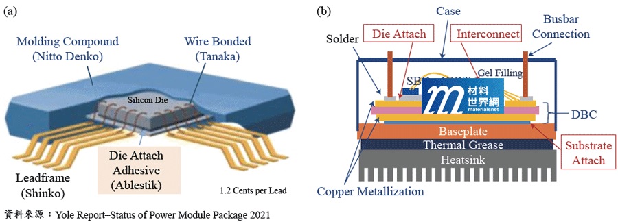
Fig. 4. (a) Power device; (b) module-packaging structure.
For module packaging—especially higher-power modules—thermal management is more critical. A common failure mode in power modules is thermally-induced cycling: mismatched coefficients of thermal expansion (CTE) cause delamination between the substrate and bonding-material layers, while gel fillers and resins inside the module that cannot withstand high temperature can fail. As shown in Fig. 4(b), in addition to wire interconnects between two chips, the chips are die-attached to a DBC (Direct Bonded Copper) substrate; the DBC is bonded to a baseplate; and thermal grease serves as the thermal interface material to the outer heatsink, creating a thermally-managed packaged module.
Silicon-carbide (SiC) industry structure
With its wide bandgap, high power density, high breakdown voltage, and good thermal conductivity, SiC is the material of choice for power devices and high-frequency substrates. Figure 7 shows the SiC industry structure, including single-crystal devices and power modules. Because SiC is used both as the main die in power modules and as an epitaxial substrate for high-frequency communications, the industry structure is divided into power semiconductors and RF semiconductors.
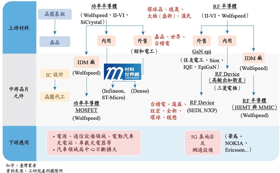
Fig. 7. Global industry structure of SiC wafers.
Leading global producers of SiC wafers for high power and high frequency include Cree and II-VI; SiCrystal is known for high-power applications. In Taiwan, GlobalWafers, WIN Semiconductors, Tankeblue (Sheng Hsin), and Hermes are active. Cree’s (now Wolfspeed) wafer sales are split between external and captive use; on the external side, Cree holds about 70% market share. ST-Micro has a long-term SiC wafer supply plan (US$220 million) and signed US$85 million 6-inch wafer supply agreements with ON Semiconductor and Infineon.
IEKView
Compound-semiconductor SiC is a key material for emerging industries spanning high frequency (5G/B5G/6G), satellite communications, IoT (smart cities), high power, and EV/xEV motors and green energy. Yet developing SiC still faces many difficulties—including downstream applications. The above is a partial excerpt; please refer to the attachment for full content.
★This article is excerpted from Industrial Materials Magazine, Issue 435. Please refer to the attachment for further details.