Technology Trends in AI Packaging Materials
As demand for AI computing continues to surge, chip design is moving toward higher bandwidth, lower latency, and greater integration, making packaging technology a critical determinant of AI hardware performance. Die-to-die interconnect technologies—Redistribution Layers (RDL), hybrid bonding, and Through-Silicon Vias (TSV)—not only boost signal transmission efficiency and density but also enable multi-die architectures in high-performance computing. In parallel, IC substrate materials are evolving by optimizing core, conductive, and dielectric properties to support high-frequency, high-speed transmission and fine-line patterning. Overall, AI-driven packaging is advancing toward high-density interconnect, low-loss materials, and high reliability, becoming a key driver of computing-platform performance.
Horizontal interconnect: Redistribution Layer
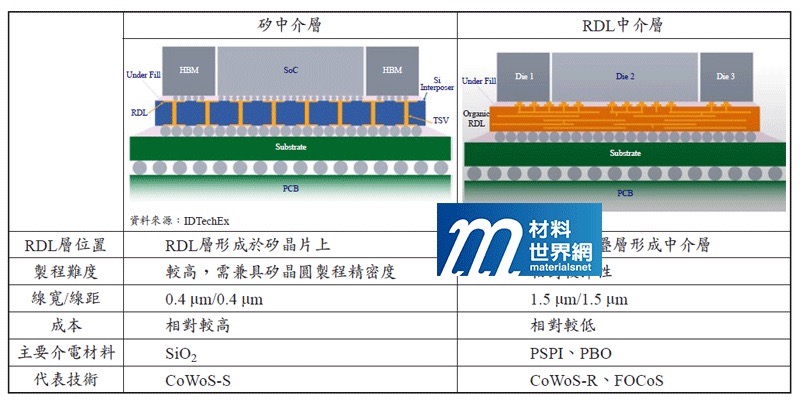
With growing AI compute demand and surging die-to-die data traffic, horizontal signal interconnects between dies are increasingly important. The key structure of advanced packaging is the horizontal interconnect, where RDLs play a core role in high-density signal routing and heterogeneous integration. An RDL is mainly composed of metal conductors, insulating dielectrics, and protective coatings. Depending on the substrate, an RDL can form either an RDL Interposer or a Silicon Interposer. Table 1 compares the two.

Table 1. Comparison of RDL Interposer and Silicon Interposer
1. RDL Interposer
The RDL Interposer replaces the conventional silicon substrate with a stack of multiple RDL layers, supporting the wiring structure with an organic dielectric rather than silicon. This approach achieves interconnect density approaching that of a silicon interposer, supports multi-chip integration, and lowers cost. The dielectric in this structure emphasizes lithographic performance and process efficiency; photosensitive polyimide (PSPI) is used because it can be exposed and developed directly after coating, eliminating extra photoresist and etch steps, shortening the process flow, and improving line resolution.
2. Silicon Interposer
A silicon interposer is built on a silicon wafer with fabricated TSVs and RDLs, providing high-speed chip-to-chip interconnect over a localized area. Unlike the organic dielectric of conventional RDLs, silicon-interposer RDLs use an inorganic dielectric—most commonly SiO2—offering low leakage, high reliability, and good thermal stability.
Vertical interconnect
2. Through-Silicon Via (TSV)
TSVs appear primarily in two contexts: TSVs in 3D packaging and TSVs in 2.5D interposers. Although both are silicon-via technologies, they differ markedly in purpose, dimensions, density, and applications. 3D TSVs are mainly used to vertically stack multiple dies—for example, memory stacks or direct stacking of logic and memory. They are typically smaller and higher-density, carrying vertical signals and power between layers, and emphasize short-distance, high-speed transmission with low latency. TSVs on a silicon interposer route signals vertically from a die into the interposer, where the RDL then distributes them horizontally to other dies or external interconnects. Interposer TSVs are relatively larger and lower-density; this structure falls within the 2.5D packaging category. Table 2 compares TSVs used in 2.5D vs. 3D applications.
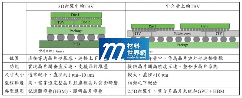
Table 2. Comparison of TSVs in 2.5D and 3D applications
★This article is excerpted from Industrial Materials Magazine, Issue 466. Please refer to the attachment for full content.